Wafer cleaning system using fine bubble cleaning for power semiconductors
Suppressing micro-cracks through ultrasonic cleaning. Supporting the improvement of power semiconductor voltage resistance with fine bubbles and ozone.
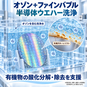
In the power semiconductor industry, it is essential to eliminate minute defects on the wafer surface and maintain high cleanliness to ensure the voltage withstand performance of products. In particular, tiny cracks that occur during the cleaning process can affect the reliability and voltage withstand characteristics of the products, making cleaning technologies that minimize surface damage indispensable. Our proposed fine bubble cleaning method efficiently removes organic contaminants and resist by using physical cleaning without ultrasound, while also utilizing ozone to reduce the load on the surface. By balancing the suppression of surface damage and cleaning performance, we support the creation of high-quality processes. 【Application Scenarios】 - Processes where the expansion of minute cracks due to ultrasonic cleaning is a concern - Improvement of voltage withstand failures caused by residual contaminants after cleaning - Resist removal and surface cleaning processes 【Benefits of Implementation】 - Suppression of surface damage through a cleaning method that does not use ultrasound - Enhanced removal performance of organic contaminants and resist through the use of ozone - Stabilization of finished product quality by suppressing crack expansion
- Company:中島物産
- Price:Other